
On Graham's recommendation, I recently bought an iCE40 FPGA and have been learning a bit about how to use it. The iCE40 is good to get because there is good open-source tooling that supports it. I was originally going to get the iCEstick evaluation board, but there are other alternatives available more cheaply and with more logic elements. I ended up getting an iceFun and have found it to be quite easy to use. The example projects are helpful.
Playing with the FPGA has led to me designing a tiny CPU, learning a bit about CPU design (in that order, unfortunately), and rekindling an old desire to build a CPU out of logic chips.
Some interesting DIY CPUs
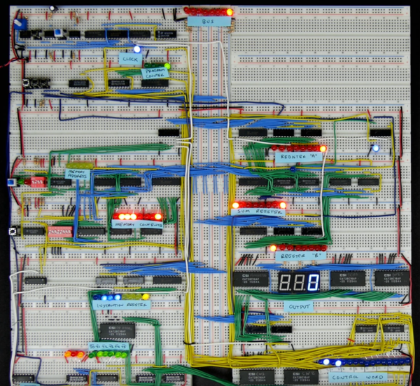
Ben Eater breadboard CPU
(Screenshot from a YouTube video).
Ben Eater has a tutorial in which he walks you through building an 8-bit CPU out of logic chips on breadboards. It's a pretty primitive CPU, sporting only 4-bit addresses (!), but it does work and is the most comprehensive tutorial I have found that doesn't resort to either FPGA or simulation.
Magic-1
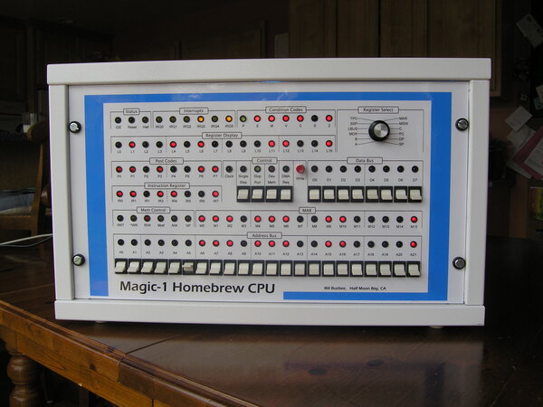
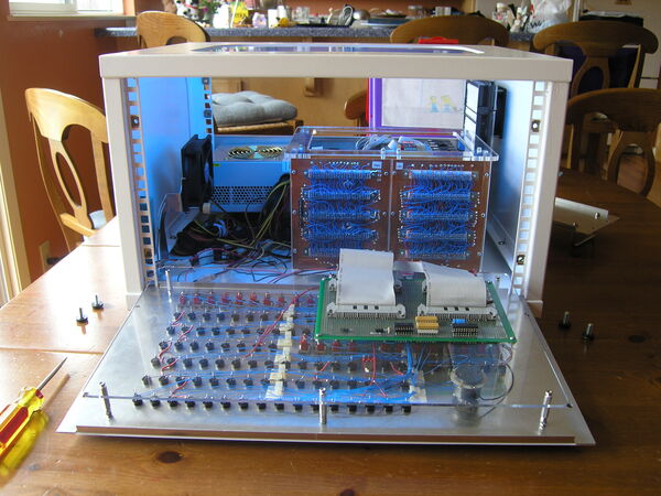
(Pictures from the Magic-1 Photo Gallery.)
I've been a fan of Magic-1 for a long time. It is the most technically-advanced DIY CPU that I am aware of (not counting FPGA designs). It has 16-bit addresses, but uses an MMU to map 4MB of physical memory into a 64K code segment and 64K data segment for each process. It also supports interrupts and memory protection, and runs a port of Minix. Really an incredible project. And it's all done with only about 200 ICs, and uses wire-wrap construction instead of soldering.
It even has a working TCP/IP stack and you can telnet to it from anywhere on the Internet. I have done so in the past but it appears to be down at the moment.
Megaprocessor
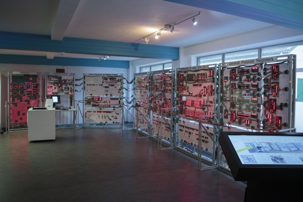
(Picture from the Centre for Computing History).
The Megaprocessor is a CPU built almost entirely out of individual transistors. Most of the transistors also feature an LED to indicate their state. It is enormous, I don't think the photograph really does it justice. It is on display at the Centre for Computing History in Cambridge, which is well worth a visit if you are interested in computing history. A lot of the computers in the museum are working and running and you're able (and encouraged!) to interact with them.
Interestingly, the Megaprocessor features four general-purpose 16-bit registers and a 16-bit stack pointer. I think if it were down to me, and I were manually building the entire CPU out of individual transistors, I might have foregone 1 or 2 of those registers, and made the remaining ones a bit narrower. But it's a brilliant machine. Has to be seen to be believed.
Using an EEPROM as an ALU
I don't know of any examples of CPUs that do this, but it's interesting nonetheless, and I'm sure there are some out there somewhere. The idea is that EEPROMs are now large and cheap enough that you can implement the ALU for an 8-bit CPU as lookup tables in EEPROMs. The "address" you look up is the concatenation of the 2 operands, and the chip you select is based on the selected operation (e.g. one lookup table for addition, one for bitwise AND, etc.).
I don't think I would go this route as it feels a bit wasteful. If you want to spend the transistor count of a bunch of 64K EEPROMs on your ALU, there are much more interesting things you can do than a lookup table. It's a funny idea though.
My first CPU
I have implemented a basic CPU in Verilog, to run on my iCE40 FPGA. I actually had almost no idea what I was doing when I started this, I was just winging it and learning as I went. And considering that there are not that many design decisions, there are quite a lot of bad design decisions.
It has an 8-bit address space, with 256 bytes of RAM synthesised directly on the FPGA, and all of the instructions take direct memory addresses as arguments. There is no support for immediate mode arguments, or general-purpose registers, or even indirect memory addresses. The reason I did this is that I thought it would keep things simple, and for the VM simulating the CPU it did. My mental model of how a CPU works is basically the same as a program simulating the CPU, which is why my first thought was to come up with an architecture that is easy to simulate, rather than one that is easy to make in actual hardware. Having written the Verilog, I now accept that it would be simpler if the operations all worked directly on registers, and there were separate load/store instructions to access memory. After all, the Verilog I wrote just loads values from memory into internal registers anyway, so they may as well be exposed.
One problem with my architecture is that the only way to support pointers is with self-modifying code. For example if you want to work with the value stored in the address stored in address 0x80, then you have to first load the value from address 0x80 into the operand of the instruction in question, so that when that instruction executes it fetches its operand from the correct address. It actually turns out to be not too hard to work with this once you've figured out the strategy, although I have not yet written any complex programs with it.
Another problem is that it forces the CPU to waste cycles on memory read/write even if the next instruction is just going to be working on the same values again.
I think a superior architecture would be to split up almost all of the separate "states" I have, and instead turn each state into an opcode: instead of "load a value from memory into a register" being a state, that should just be the total effect of an instruction. That way the programmer has more control over the work the CPU is doing, instead of having to select from a tiny array of available opcodes and then watch the CPU stupidly storing at, and loading from, the same address over and over again.
The biggest problem with my CPU is that I don't fully understand some of the timing problems. I added a "wait" state that allows it to waste some cycles while waiting to get data back from RAM, but I found that if I make it wait for between 2 and 22 cycles, then the CPU sometimes gets into an illegal state and halts. I do not know why. If I only wait for 1 cycle then it always works, and if I wait for 23 or more cycles, it always works.
(Update 2021-01-15: Graham pointed me to a comment in nmigen which suggests there is a hardware bug in the iCE40 FPGAs that means block RAMs read all zeroes for the first 3 microseconds. Fun. The solution is to make the CPU sit idle when it first starts up for long enough to let the RAM start working. The reason my CPU sometimes worked before is that opcode 0 is NOP! As long as RAM was returning all zeroes, it would just sit and NOP forever. I think the problems arose in cases where it was trying to fetch an instruction across the boundary of the memory starting to work. It would get a correct opcode, but an incorrect operand, which would eventually lead to trying to execute an illegal instruction and halting.)
Nand2Tetris
Since working on my Verilog CPU, I have gone through the Nand2Tetris part 1 course. "Part 1" is hardware design and "part 2" is software design, I've only done part 1. The course is taught using a dedicated hardware-description language, with a basic Swing GUI, called "HDL". HDL differs from "real-life" hardware-description languages mainly in that it supports almost no syntactic sugar, which means you are forced to understand everything from first principles. It has a builtin NAND gate, and a builtin D-flip-flop, and you make everything else out of these primitives. (The course does explain that in real life D-flip-flops can be made out of NAND gates, but the hardware simulator in the course does not support cycles in the graph of gate connections, so D-flip-flops are provided as a special-case primitive).
You start by making basic logic gates out of just NAND, then combine them together to make logic gates that operate on a bus (e.g. 16-bit AND), then create multiplexers and demultiplexers, a half adder and full adder, an ALU, rewritable storage elements starting from a single bit and building all the way up to a 16K-word RAM, and a memory implementation that includes the RAM and the memory-mapped IO. The CPU itself is actually extremely simple once all of the supporting pieces are done.
Following the Nand2Tetris course gave me a much greater appreciation for what is going on when I write Verilog.
The course is meant to be accessible to someone who has no prior knowledge of computer science, so if you have prior knowledge then you can skip over the parts of the lectures that you already know and just complete the exercises. I thoroughly recommend the course, I learnt a lot from just doing the exercises, and watching the lectures on the parts I didn't understand.
The CPU they have you design uses a 16-bit address space with 16K-words of RAM, and then 8K-words of memory-mapped IO for the screen, and 1 word of memory-mapped IO for the keyboard. Each instruction is a single word, and there are 2 types of instruction: "A-instructions" load an immediate 15-bit value into the A register, and "C-instructions" compute something using the ALU. Various bits in the opcode specify where the 2 inputs come from, where the outputs go, how to operate the ALU, and whether to perform a conditional or unconditional jump.
The biggest revelation for me in Nand2Tetris was the design of the ALU. The core of the ALU is just a 16-bit adder, and a 16-bit bitwise AND. There is a flag to select the function (add or AND), and there are flags to zero out each of the inputs, and invert the bits of each of the inputs, and a flag to invert the bits of the output. Unbelievably, using just the adder, the bitwise AND, the 2 zero flags and the 3 negation flags, the ALU can compute quite a lot of different functions:
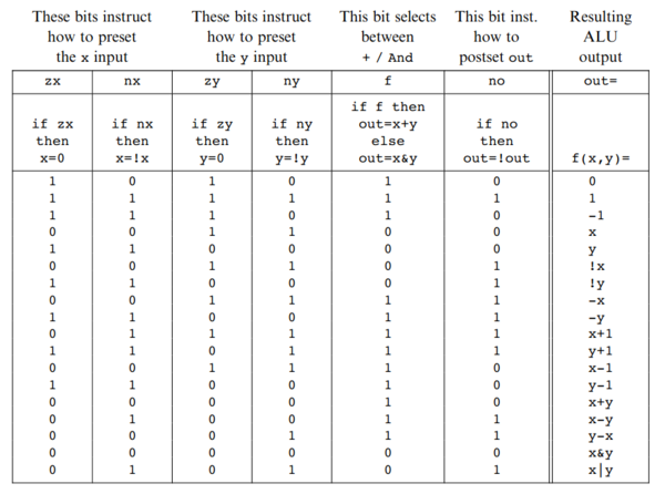
(From the course textbook).
I think this ALU (and the entire Nand2Tetris instruction set architecture) is really beautiful in its simplicity.
The only thing I didn't like about the Nand2Tetris CPU is that it uses the "Harvard architecture", i.e. it separates code and data. The code is stored in a ROM, and there is no way to execute code in RAM, so this means the CPU is wholly incapable of creating and running new code. You can't make a bootloader, and there is no chance of running any programs that you compile within the CPU, without going through some external system to write them to the ROM. The reason they have done it this way is it means the CPU doesn't need an internal state machine: at each cycle it gets a 16-bit instruction from the ROM and a 16-bit value from RAM, and can operate on them both simultaneously, without even having to toggle between "fetch" and "execute" states.
My next CPU
I would like to design a simple CPU that I can create using discrete logic chips and use to run a CP/M-like OS. Although the ultimate goal would be to physically build the CPU, I would start with an FPGA because that makes it a lot easier to iterate and debug.
It should be as simple as possible, while still able to run an OS. In all but the most extreme cases, I would rather trade off performance to gain simplicity. I think I would probably want to support interrupts, but this might just be in the form of a single global interrupt handler, which is then responsible for polling the attached devices to work out which one of them wants to do something. Not completely sure on that.
I think I would save the bother of breadboarding or wire-wrapping, and get PCBs made in China.
I would abandon the memory-to-memory architecture of my first CPU design, in favour of a more traditional register-based architecture, and I would almost certainly copy the Nand2Tetris ALU.
I would want the OS to be self-hosting, and I'd want it to be able to run a compiler for either C or a C-like high-level language, although the OS itself would probably be written in assembly language. There are a decent handful of C compilers available for CP/M, so it is clearly possible to run a C compiler in such an environment. Interestingly Magic-1 can not run a C compiler, I'm not really sure why. The only way to compile C programs for Magic-1 is to cross-compile them from a more capable machine.
(Update 2021-01-31: In Bill Buzbee's latest video on Magic-1 he reveals that it now compiles something called "Small C" natively. I expect this is a relative of this smallc compiler I found on github. I expect that might be worth trying to use for my CPU as well.)
I'd probably want a 16-bit address space, but I'm still undecided on whether I would want 8-bit or 16-bit words. 8-bit words probably result in less circuitry required overall, but they do complicate the state machine of the CPU because addresses would have to be read in 2 separate fetches from memory. Perhaps it might be funny to have an oddball word size that's not a multiple of 8.
In terms of the rest of the computer, I think I'd be looking for roughly RC2014-level capabilities. So I'd want a serial console, a second serial port for other communication, and some sort of storage (probably either hard disk, CompactFlash, or SD). Since I already know that this is what I want, I don't think it would be too hard to make it compatible with the RC2014 bus so that in a lot of cases I could use unmodified RC2014 cards.
I don't think I would want to support bank switching. It seems like the RC2014's bank switching is rather wasted on CP/M, as CP/M programs don't know how to use it. I think I'd aim to have a very small boot ROM that is permanently mapped into the address space, and that just presents a basic boot monitor and loads the OS off the storage device.
I don't know how likely this project is to happen any time soon, but the idea of making my own CPU has intrigued me ever since I first saw Magic-1, and I'm definitely now closer than ever to being able to make it happen.