
I'm pretty happy with the CPU design now and am ready to proceed to making it physically exist. I am still finding the odd microcode bug, but these can be fixed at any time. I'm at least not finding any architecture-level bugs.
Physical organisation
I think I want a metal box with a backplane at the back, and cards that slide in from the front. One of the mistakes I made with my RC2014 build is that I put all the electronics inside a metal box with no way to access them without opening the case. This makes hardware modification dramatically less convenient than if you just have the RC2014 cards directly accessible. So for SCAMP I definitely want to be able to slide the cards in and out without tools.
I was also thinking that I might implement the "front panel" as 3d-printed mini-front-panels directly on the cards. For example, the card that holds the instruction register would have LEDs at the front that indicate the contents of the instruction register, rather than having wires running to LEDs on a separate panel.
And I think I've had quite enough of manually entering code using switches on the front panel, so I don't think I need to support that. All I really want from the front panel is single-stepping, clock speed control, and blinkenlights.
I considered using card-edge connectors to connect the cards to the backplane, but I've never used them before, and it seems like it would be easy for me to accidentally get the PCBs made in the wrong thickness, or with the wrong plating, or something else, and then they wouldn't connect properly. I thought it more prudent to just go for pin headers for the backplane connection.
By the way, if you are trying to buy female pin headers on Farnell, then you need to look in the "PCB Receptacles" category.
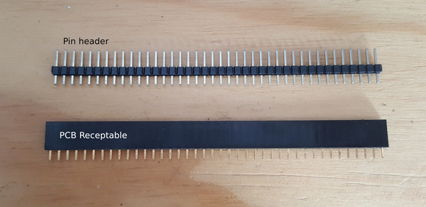
I'm planning to use 2x30 pin headers, with male headers on the backplane and female right-angle "receptacles" on the cards. I thought it best to put the male side on the backplane, because pins are more easily damaged than sockets, and it is likely that they'll be better-protected inside the chassis than loose on the cards. I'm thinking I'll have some guide rails in the sides of the chassis that guide the receptacles directly onto the pins, to avoid misalignment.
I haven't completely decided how I'll arrange the logical modules of the CPU into cards, but it'll be something like:
| Card | Modules | Chips |
|---|---|---|
| ALU | ALU, X register, Y register, flags register | 43 |
| Memory | ROM, RAM, address register | 9 |
| Instruction | Instruction register, microcode ROM, control logic, sequencer, program counter | 22 |
| I/O | UART, CompactFlash, SD card | ? |
| Clock | Clock circuit, single-stepping, reset button, power switch | ? |
ALU cards
Concept
I'm starting with the electronics for the ALU because it will be the most complicated. I'll then know that whatever PCB size I end up with, as long as I can fit the ALU on it, I should be able to fit the others in the same amount of space.
In the TTL-Verilog implementation, I split up the function of the ALU into 4-bit slices, and then used 4 copies of this to build the 16-bit ALU. Similarly, the X and Y register are each naturally implemented with 2x 8-bit-wide 74377 register chips.
It is therefore natural to split the ALU into 2 physical cards. One card would implement the low 8 bits and the other would do the high 8 bits. We don't even need to transfer bus or register contents between the 2 cards. Each card already has its own connection to the bus, and takes its control signals from the bus, and neither card needs access to the register bits that are stored on the other card. We just need a flying jumper between the cards to pass the carry bit up. The minimum order from JLCPCB is 5 boards, so needing to buy 2 copies of the card doesn't even cost any more money, and in fact saves money because the resulting PCBs are smaller.
We also need the flags register to be implemented on the ALU cards. It is sufficient to leave the footprint for the flags register on both cards and only populate it on one. Part of the flags register calculation is checking whether the ALU output is 0, so we need a second flying jumper to pass the "zeroness" check of the secondary card up to the primary card.
Finally, to connect up the 2 cards to the upper or lower bits of the bus, I'm using solder jumpers. On one card the 8 solder jumpers would be connected to bus[0]..bus[7], on the other card they'd be connected to bus[8]..bus[15].
In terms of physical packaging, I'm planning to screw the 2 cards together using a standoff which spaces them apart to match the connector spacing on the backplane. They'd use a shared 3d-printed front panel piece, which would present convenient views of the X and Y register, flags register, ALU operation selection, and ALU output. Something like this:
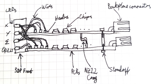
Not my proudest sketch, but it perhaps communicates the idea. The front panel is a 3d print that houses the LEDs. The LEDs are plugged into pin headers directly on the cards (with 8 bits of X,Y from the top card and the other 8 bits from the bottom card). Then the cards are each populated with the chips required to implement their logic, with a couple of flying jumpers to pass extra bits between them, standoffs to hold them together, and a backplane connector at the back of each card.
Implementation
I have made a start on the PCB design, but there is still some stuff I want to change. Here's what I have so far:
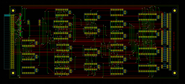
(Just to keep you on your toes, this picture has the backplane connector on the left instead of the right, compared to the sketch).
This time I made a point of routing horizontal traces on one side of the card and vertical traces on the other. I think I got the idea from an EEVBlog video, but I don't remember which one. It is a great idea because it makes it a lot easier to route the last traces if you can always predict where you're able to go without crashing into things. I still used KiCad's push-and-shove router, which is clearly the best way to route traces and I don't know why it is not the default.
I did notice one issue with the push-and-shove router: sometimes, if you're routing a long trace, you can get it to a point where you want to drop a via, hold the mouse still, and press "V" to drop the via, but as soon as you press "V" it looses its route and you have to start again. I don't know why. The trick is to click just before you drop the via to lock in the route you have so far so that it can't go anywhere.
The PCB is about 103 mm tall and 237 mm wide. It could clearly be smaller, but I don't know if it's worth starting again to make it smaller.
Other
EEPROM
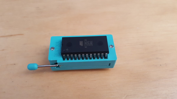
The logic chips are mostly going to be fitted in normal DIP sockets, but for the boot ROM and microcode ROM, I'm going to be using Zero-insertion force ("ZIF") sockets, to avoid bending the pins.
I bought 4x Atmel AT28C16 EEPROMs from eBay. They arrived packaged like this:
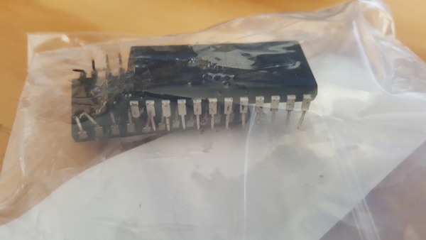
So much for not bending the pins...
I have manually straightened out the pins and miraculously none of them have broken off, but I'm not sure how many insertions I can expect before they fail. The pins are also very corroded, as if they have been stored outdoors for several months, despite being sold as "New".
I still need to make an Arduino-based EEPROM programmer, but I don't expect that will be difficult.
The AT28C16 chips each store 2 KBytes of data. For the boot ROM I only need 256 Bytes from each one, but I couldn't find any convenient smaller EEPROMs and these weren't too expensive, so I don't mind wasting the rest.
RAM
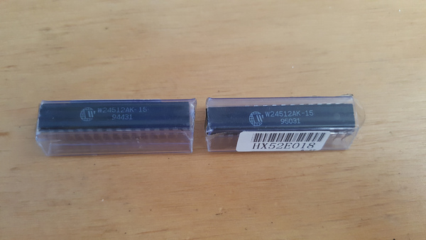
For RAM I'm going to be using 2x Winbond W24512A chips. These are each 64 KBytes of RAM, together providing 64 KWords. The lower 256 words will not be accessible because the EEPROM will be mapped there. But again I don't mind wasting this space.
The RAM chips were packaged much better than the EEPROMs:
UART
I wanted to use a MOS 6551 for the serial port, because (almost uniquely, it seems) it has an onboard clock source to provide the baud rate.
One of the things I don't like about the RC2014 is that the baud rate of the serial ports is derived from the CPU clock, which means if you use a slow clock, your serial terminal doesn't work properly. I'm keen to avoid this.
Unfortunately the 6551 is pretty hard to find, and I couldn't find any available on Farnell, RS Components, or eBay. So that rules that out.
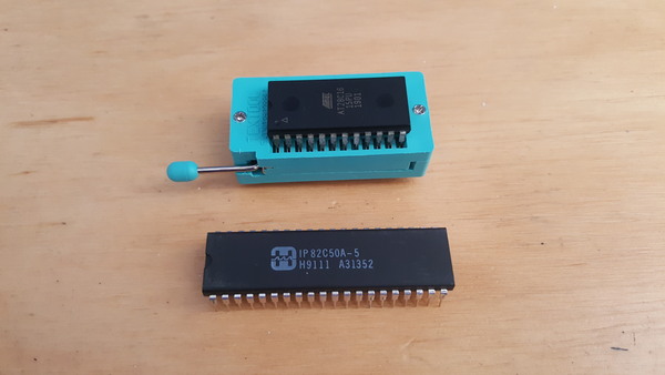
The next best option that I could find is the National Semiconductor 8250 (now cloned by lots of other companies). This is the chip used in the original IBM PC to provide the serial ports. It requires an external clock source, which is potentially annoying, but does at least have quite a wide-ranging internal divider to allow different baud rate selection in software.
It is quite a big chip, here it is next to the EEPROM, which is itself not small:
I have only bought one so far. I definitely want one to use for the console, and probably once I am satisfied that it is going to do what I want I will buy a second one to use for SLIP networking or talking to Arduinos.
To implement the serial console, I probably want to get something like Geoff's VT100 Terminal Kit.
Storage
I am not yet sure what I'm going to be doing for storage. The obvious candidates are to use a CompactFlash card or an SD card. I think using an SD card in SPI mode would be an unnecessary performance bottleneck (especially if I want to support a "process stack" system() implementation that swaps the running process out to disk to execute a child process). But I understand that the easiest way to use a CompactFlash card is in IDE mode, and if I'm going to be supporting IDE then it's cooler to buy an old hard disk and use that instead.
But supporting an SD card as secondary storage might be useful for exchanging files with other computers. I'd really like to be able to do this year's Advent of Code on SCAMP, and an SD card would be a convenient way to get problem inputs onto the computer, and finished programs off.
FPGA CPU
I've now got an FPGA implementation of the CPU. I initially thought this would be relatively trivial, but it turns out that FPGAs don't really like tri-state logic. My solution was to replace all of the tri-state bus-driving logic with a single big mux that sets the bus contents based on whatever should be driving it. The FPGA I have also doesn't have enough space to store 64 KWords of RAM, so a lot of the RAM is just a black hole in the FPGA version.
But it does work, and I have been able to write a program that tests the state of the buttons on the evaluation board, and mirrors this over to the LED array. I accept that it would probably be less code if it was written directly in Verilog, but it serves its purpose as a CPU test.
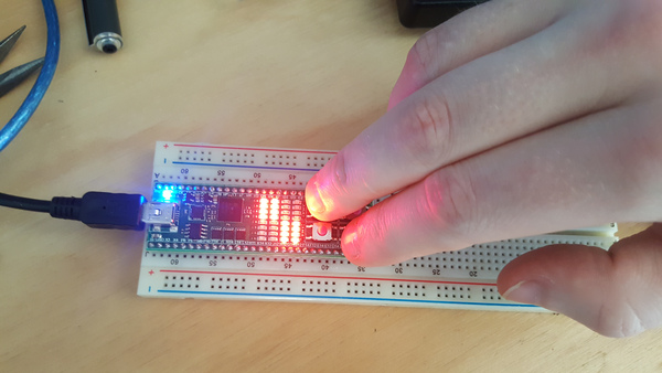
I exposed the buttons as input device 0 (so when you ask for input from device 0, the lower 4 bits are set or not based on whether the corresponding button is pressed or not), and the LEDs as 4 output devices (the lower 8 bits of the data written to device 0 goes to the first row of LEDs, etc.).
My initial motivation for the FPGA implementation was that it would allow me to test external hardware "piecemeal", by just deleting the corresponding Verilog and connecting its inputs/outputs to some physical pins. Unfortunately I now realise that won't work, because the CPU I'm making is all going to run on 5v logic, and the FPGA only supports 3.3v. Never mind.
Oscillocopes, logic analysers
I currently have a "JYETech DSO112A", which looks like this:
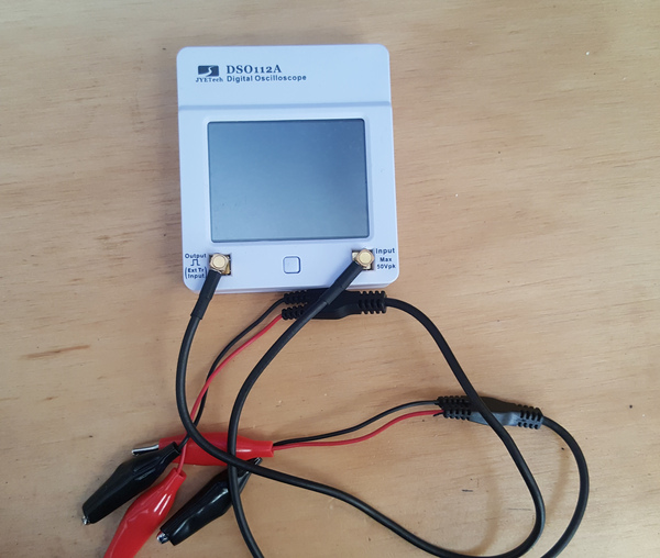
It sucks, and I am kind of in the market for something better. The Rigol DS1054Z comes relatively-well recommended, but it seems quite proprietary, and for example some features from a more expensive model are locked behind a software gate. I want to use software that helps me as much as it can, not software that views me as an adversary to its master's business model.
It also seems to me that even the best user interface on a physical oscilloscope wouldn't be able to beat a proper keyboard-and-mouse GUI, and I expect it would be possible to make a better oscilloscope for less money if the "data collection" part were performed by dedicated hardware and the "presentation" were performed on a PC. But it seems like all of the scopes that work this way are considered inferior, I don't really know why.
So if you have any recommendations for oscilloscopes or logic analysers that you think I might like, please email me. I'm not averse to a hardware UI, but I am quite averse to proprietary software.